The CS Hub is structured around 4 academic centres, supported by a variety of industrial partners, delivering 8 work packages and 2 grand challenges in compound semiconductor manufacturing. The delivery of the research of the CS Hub is overseen by a management strategy which includes a Management Board, a Strategic Advisory Board, and an Industrial Advisory Board.
Platform funding will be used to:
1) Develop Silicon like manufacturing processes for CSs,
2) Develop the manufacturing of CS grown on silicon for integrated functionality and dramatically reduced cost.
Platform Funding
To date the remarkable capabilities (e.g. light emission, higher speed, etc. c.f. Si) of III-As, III-P and III-Sb compound semiconductors have been achieved by growth on small area native substrates and, in almost all cases, bespoke device fabrication processes for particular applications.
By contrast the successes of Si electronics have been due to a foundry approach, where devices are created from a suite of common fabrication processes on large area substrates. This facilitates the advantages of mass production even for smaller scale applications, as suitable structures can be developed on a large shared substrate.
With support from Industrial Colleagues, we will begin the process of developing a foundry type approach for GaAs based compound semiconductors on native substrates and Si and for GaN based compound semiconductors grown on Si and SiC, which is even more challenging because of defect formation due to lattice mismatch and thermal expansion mismatch. In III-Ns, where a native substrate is not available at any suitable scale, progress has been demonstrated using growth on mismatched substrates. A fundamental reason for the success is thought to be Indium segregation and consequent localisation effects preventing carrier diffusion to defects and associated non-radiative centres.
Progress in devices using quantum dot active regions in III-As materials grown on Si also relies on carrier localisation to produce excellent performance. This coupled with recent developments in nanowires (which can accommodate the lattice mismatch) and selective area growth make it extremely timely to develop growth of compound semiconductors on Si. This paves the way for the integration of different compound semiconductors on the same substrate and the integration of compound semiconductor functionality with that best obtained using Si. In some applications, e.g. those requiring radiation hardness or operation at high temperature, it is better to integrate on a compound semiconductor substrate e.g. GaAs, where 150mm growth and Si style fabrication needs developing.
Progress in the growth of compound semiconductors on Si has proceeded somewhat in isolation and have produced essentially different optimum solutions for the interface between III-Sb, III-As and III-N and silicon. With the scale and expertise in the CS Hub we will develop more effective, combined solutions for III-Vs on Si.
Choice of Hub and spokes
- Sensors and communication are essential to the emerging application megatrends
- Building on world renowned research excellence Cardiff University invests in capital and academic staff excellence
- Spokes complement, with world leading scientific and manufacturing excellence in
- GaN on Silicon (Sheffield), lauded by Nobel Laureate Nakamura,
- The first practical compound semiconductors on Si Lasers (UCL) and
- Reproducible, high tolerance compound semiconductor manufacturing and
- Its inclusion in partner supply chains (Manchester).

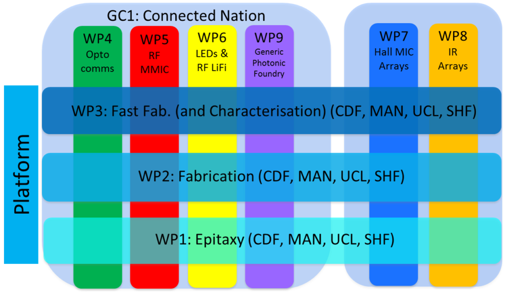
Work Package Structure
Grand Challenge 1: GC1 Enabling the connected nation
Grand Challenge 2: GC2 Sensing
WP 2: CS on Si device fabrication
WP 3: Fast Fab – Integrated growth, fabrication and characterisation
WP 4: Manufacturing technology for optical datacommunications on Si
WP 5: Advanced RF devices and MMICs
WP 6: Monolithic integration of RGB LEDs and integrated RF electronics for LiFi
Management