
Recently, high performance silicon based InAs /GaAs quantum dot (QD) lasers have been demonstrated with CW operation at high temperature (>75oC) and long lifetimes (>100 000 hours) by UCL and Cardiff. Here we will further develop our world leading III-V-on-Si technologies to create high performance lasers and semiconductor optical amplifiers (SOAs) for data communications applications.
Lead: Prof. Huiyun Liu (huiyun.liu@ucl.ac.uk)
Contributing Academics: Dr Mingchu Tang, Dr Siming Chen, Dr Qiang Li, Dr, Samuel Shutts, Prof. Alwyn Seeds, Prof. Peter Smowton
Overview: The present work package has been dedicated to continually advancing silicon-based InAs/GaAs quantum dot (QD) lasers to further improve the superior performance. This report highlights the recent strides in promoting the InAs/GaAs QD lasers’ performance through doping methods. In addition to the conventional n-type and p-type doping methods, a novel co-doping approach has been introduced to reduce the threshold current density while maintain the high-temperature performance.
In this package, we have made significant enhancements to the performance of 1.3 μm InAs/GaAs QD lasers by employing doping techniques. Building upon the QD characteristics previously observed, characterised by an ultra-high dot density (>5.0 x 1010 cm-2) and high uniformity, we have successfully achieved low threshold current density and good high-temperature performance by employing both p-type and n-type doping. The novel co-doping approach combines both p- and n-type doping methods to retain the advantages of individual doping techniques while surpassing their performance capabilities.
Progress and Challenges: The usage of InAs QD as the active region for lasers on Si substrate has attracted attention since it can potentially reach the “holy grail” for Si photonics. However, the high threshold current for InAs QDs, particularly due to the highdensity of threading dislocations on Si substrates, remains a notable concern. Apart from the threshold current density, the poorhigh-temperature performance is another concern due to the closed-spaced hole in the valence band. Studies have indicated that the p-type modulation doping method offers several benefits, such as increased characteristic temperature at high temperatureswith enhanced model gain. In comparison, the direct n-type doping method is proven to increase the emission intensity anddecrease the threshold current of QD lasers. To preserve the advantages of the sole doping techniques, a novel co-doping methodhas been applied to the active region by introducing Si and Be dopants directly to QD active region.
Figure 1 (a) shows the threshold current density of undoped, solely doped and co-doped QD lasers at the temperature range from27 to 97 ℃. The threshold current density drops to 50% of the undoped lasers through the novel co-doped method. To the best of our knowledge, this is the most effective method to decrease the threshold current density without considerable modifications tothe laser structure or fabrication process. In addition, it also preserves better high-temperature performance as p-type modulationdoping. Figure 1 (b) shows the temperature-dependent L-I curves for the co-doped laser with a 2-mm length under CW operation.The insert of Figure 1 (b) gives the single-facet output over 100 ℃ for the co-doped QD laser, while other lasers failed to laseover 100 ℃ under CW operation.
In summary, we successfully demonstrated a significant reduction in threshold current density by implementing our novel co-doping method during laser growth while maintaining the increase in the characteristic temperature and improvement in the highest operating temperatures due to p-type modulation doping. These findings suggest that our novel doping method holds great promise in advancing InAs/GaAs QDs towards achieving the highly sought-after Holy Grail for Si Photonics [J. Phys. D: Appl. Phys. 55.21 (2022): 215105)].
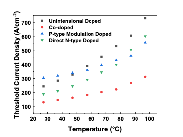
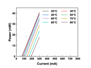
Figure 1. (a) Laser performances at different temperatures threshold current density for the undoped, p-type doped, direct n-type doped and
co-dopedlasers at the temperature range from 27 to 97 oC. (b) The single-facet laser
output of co-doped QD lasers with 2-
mm length at the temperature rangefrom 20 to 130 oC under CW operation.