
The aim of Work Package 9 is the development and progress of generic photonic integration in optoelectronics devices and systems. Photonic integration allows multiple optical devices to be fabricated on a single chip, which in turn aids the realisation of monolithic integration technologies in addition to the smaller size, lower cost and higher efficiency and reliability. Overall, photonic integration technologies drive the development of next generation high performance devices for data communications and biomedical applications
Lead: Dr Yun Long (longy11@cardiff.ac.uk)
Contributing Academics: Peter Smowton, Huiyun Liu, Michael Wale, Lalitha Ponnampalam, Pawan Mishra, Fwoziah Albeladi, Sara-Jayne Gillgrass
Overview:
Photonic Integrated Circuits (PICs) have proven to be the driving technology behind next-generation high performance devices, due to their advantages including miniaturisation, higher speed, large integrating capacity and compatibility with existing processing flows which allows for high yield and volume manufacturing. Our approach to optoelectronic integration is based on a quantum dot active material, which must enable a variety of active functions such amplification and detection, along with passive functions such as waveguides, splitters and combiners. Quantum dot material is suited to producing emission and absorption over a wide wavelength range while operating a relatively low current. Progress is also required on passive functions aimed at solutions to reducing loss. We have been working with selective area intermixing approach by using ion bombardment and strain induced intermixing. Our experiments resulted in an overall blue shift of approximately 155 nm with SiO2 capping and annealing at 725°C compared to the as-grown sample. Additionally, by using Ta2O5 and SiO2 as capping layers in different areas of the chip, we achieved an overall spatial blue shift of about 60 nm on the chip through RTP at 675°C. (Figure 1)
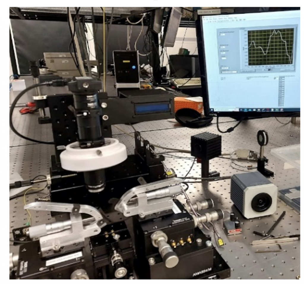
Silicon is one of the most popular materials used for manufacture of Photonic Integrated Circuits (PICs) due to its abundance, thermal and chemical stability, ease of manufacture and the existing manufacturing infrastructure. InP based photonic integrated circuits on the other hand have the benefit of intrinsic active building blocks although other aspects are not as favourable. In WP9 we are exploring the relative advantages and the practicality of manufacturing an integrated subsystem for Optical Coherence Tomography (OCT). We are currently investigating the use of the GaAs-based platform whilst comparing and contrasting with work done on an associated project on silicon/silicon nitride in addition to published work using InP. Within the integration process, a broad range of functionalities can be realised from basic building blocks (BBBs) which control light propagation. A variety of circuits and systems can be realised through connection of these building blocks in a variety of topologies, a process known as generic photonic integration. In chip design, generic integration processes can be enhanced through the development of a Process Design Kit (PDK) with component libraries containing accurate models of building blocks, which will lead to a reduction of the design time and costs necessary to achieve the required performance. In the past year work has progressed towards designing a Silicon-Nitride based tunable laser, which comprises a set of basic building blocks designed using Photon Design software. The building blocks designed for the Silicon platform will also serve as the basis for a Process Design Kit for optoelectronics systems based on a GaAs platform. In addition, the assembly of a software controlled experimental setup has been completed (Figure 2), which uses the technique of Grating Coupling – a technique involving optical fibres positioned directly above the chip – to measure coupling efficiency in passive waveguide devices. This technique has advantages which include compact size, wafer-level testing capability and flexible coupling position which allows more leeway in circuit layout and has a greater tolerance to alignment errors.
Progress and Challenges:
- Construction of test bed for measuring optical output in passive building blocks and integrated circuits.
- Re-finalised list of requirements for PDK towards the realisation of an OCT system based on Silicon/Silicon Nitride.
- Design and simulation of reflectivity spectra for basic building block comprising tunable laser on Silicon Nitride using Photon Design.