This work package is addressing the key challenge of growing high quality compound semiconductor layers In many cases this involves growth on to substrates with large lattice mismatches A particular focus is the growth on to Si substrates to allow, low cost, large volume manufacturing of the devices being developed with in the Manufacturing Hub
Lead: Prof David Wallis (WallisD1@Cardiff.ac.uk)
Contributing academics: Tao Wang (Sheffield), Mo Missous (Manchester), Huiyun Liu (UCL), and Qiang Li (Cardiff). Although no longer funded by the Manufacturing Hub, we also maintain close contact with the work of Prof. Manus Haynes (Lancaster) and Dr Philip Shields (Bath), both of which were recipients of Future CS Hub sponsored feasibility studies. Both groups have won further support for the projects started under the Hub funding and continue to work with the core partners of the Hub.
Overview: Work package 1 brings together all the compound semiconductor growth activities being undertaken with in the Future Compound Semiconductor Manufacturing Hub. This covers a diverse range of materials systems, including Nitrides, Arsenides and Phosphides. A key focus of this work is the growth of device structures on to substrates that are compatible with, low cost, large volume manufacturing to allow exploitation of the technologies developed in commercial markets.
Progress and Challenges: Putting the COVID restrictions behind us, good progress has been made across all the materials technologies being developed in the Hub. Work this year has included the upgrading of the many of the growth capabilities along side development of the growth technologies. Some examples of the developments achieved are described below:
One development from Prof. Tao Wang at Sheffield has been the growth and processing of porous semi-polar GaN layers that can be used as Distributed Bragg Reflectors (DBR) in LED devices. The porous GaN layers allow much larger refractive index contrast than can be achieved in bulk Nitride layers and therefore give mirrors with almost perfect reflectivity. This helps significantly with the light extraction from resonant cavity LEDs increasing their performance and efficiency.
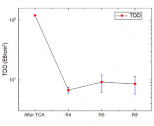
Another development funded by the CS manufacturing Hub in Prof. Liu’s lab at UCL is the development of new InGaAlAsasymmetric graded structures (ASG) for the filtering of threading dislocations. These graded composition layers allow GaAs structures to be grown on to Silicon substrates with threading dislocation densities (TDDs) as low as 7×106 cm-2 . Since threading dislocations are a major cause of degradation in GaAs based III-V lasers on Silicon substrates this development could significantly enhance their performance allowing the integration of III-V photonic devices with Si electronics