Recent technical and scientific challenges have involved fast fab of vertical cavity surface emitting lasers (VCSELs); scaling up characterisation for optical devices using auto probe wafer mapping reporting degradation mechanisms of III V lasers on Si, testing and expanding existing device degradation studies and developing fabrication and measurement techniques for mode locked lasers.
Lead:Dr Craig Allford (AllfordCP1@cardiff.ac.uk)
Contributing Academics: Prof. K. Elgaid, Dr Q. Li, Prof. H. Liu, Prof. M. Missous, Dr R. Quaglia, Dr S Shutts, Prof. P.M. Smowton, Prof. D. Wallis.
Overview: This work package is focussed on developing novel fast fabrication and characterisation approaches using simplified devices and reduced fabrication processes to provide valuable rapid feedback on device performance, fabrication, design and epitaxy. Establishing and scaling up these approaches to large diameter (>100mm) wafers and disentangling the effects of fabrication from device performance in a reduced time frame can minimise the development cycle, improve product yield and reduce manufacturing costs.
In this period we have established capability for the wafer-scale characterisation (up to 200mm diameter) of etched-facet edge emitting lasers, including Light-Current-Voltage (LIV) and spectral properties of quantum dot and quantum well based lasers operating at 1310nm and 1550nm respectively. We have further expanded our on-wafer characterisation capability with the acquisition and integration of a pulsed laser diode current source (0-5000mA, 500ns to 5ms), high resolution (900nm-1700nm) and high sensitivity (200-1000nm) spectrometers, in addition to a wide-beam imaging system for on-wafer testing of Vertical Cavity Surface Emitting Lasers (VCSELs) and Light Emitting Diodes (LEDs). A system for the characterisation of ultra-fast light pulses (50fs to 40ps, 700-1600nm, up to 30 GHz), such as those generated from passively mode-locked lasers, has also been developed.
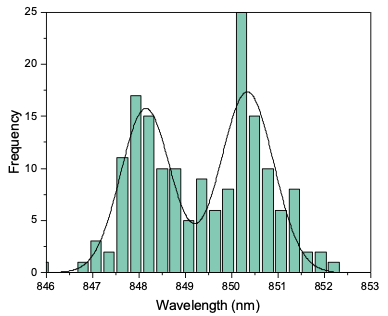
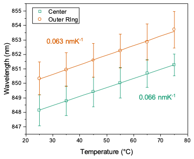
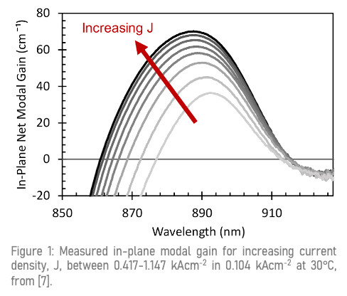
Progress and challenges: Highlights in this period include the previously developed VCSEL Quick Fabrication (VQF) technique exploited to investigate effects of VCSEL growth and fabrication on GaAs and Ge substrates. VQF is also a powerful tool for the rapid fabrication, characterisation and feedback to epitaxy it has been utilised for the characterisation of VCSEL epitaxial wafers designed for quantum applications such as atomic clocks and magnetometers. Additionally, a novel technique for the direct measurements of optical gain in VCSEL material using the segmented contact technique has been pioneered by CSHub researchers.
We have also continued to develop quantum-dot based edge emitting lasers operating in the C-band (1550nm) for next generation light detection and ranging (LiDAR), telecommunications and photonic integration applications. Presented at the IEEE Photonics Conference 2022, held in Vancouver, Canada, this work demonstrates the excellent promise of this technology for delivering high performance optical source for integration onto silicon substrates via a direct epitaxy approach.