PhD Opportunity: Development of Integrated Optic Devices for Harsh Environments
 The fast maturing field of Silicon Photonics research is already being transferred to industry applications by some of the leading technological companies including Intel, IBM, Hewlett Packard and Cisco. Primary industrial use of this technology is in optical interconnects for datacom/telecom applications. Silicon Photonic systems are also used in harsh environment applications (aerospace, naval, and nuclear industries) with a ruggedized package. Due to its defect-tolerance, temperature and radiation hardness, GaAs-based electronics is the dominant material in harsh environments. This PhD will develop the use of GaAs-based materials in photonic devices and systems in order to further improve the performance and lifetimes of devices and systems towards a better scalability and manufacturability standard for systems in harsh environments.
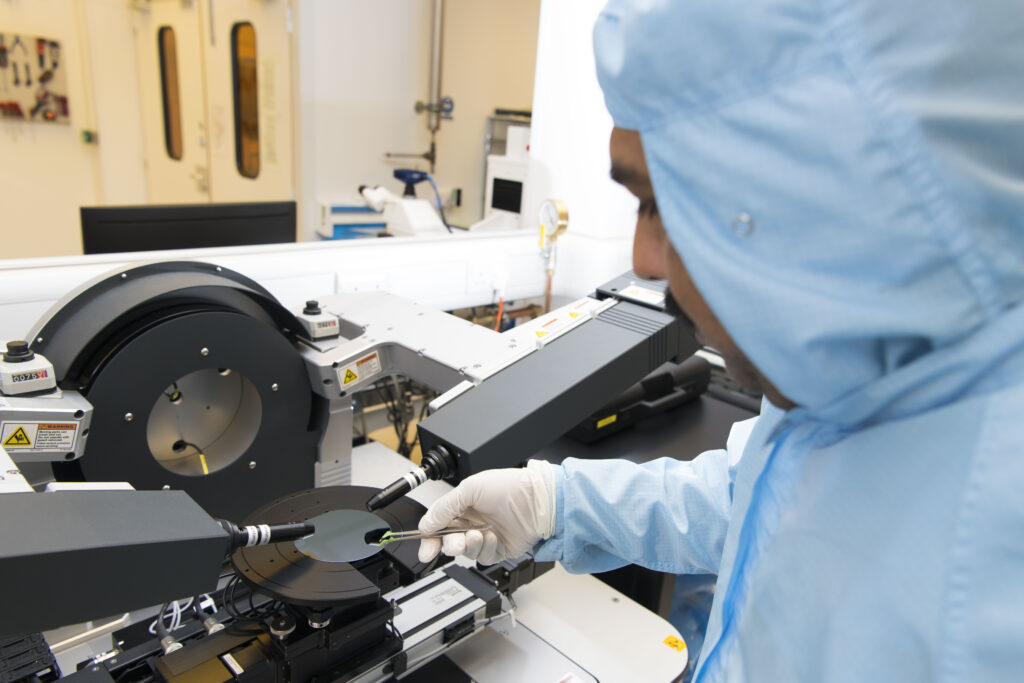
The goal of this PhD is to invent and develop the proof-of-concept of GaAs-based devices for use in harsh environments. The student will work within the framework of the Future Compound Semiconductor Manufacturing Hub (CS Hub, www.compoundsemiconductorhub.org/), which comprises 35 industrial partners and 4 universities, with the objective of developing compound semiconductor research from materials to systems. Among the industrial companies involved in the CS Hub, Oclaro, Kaiam, Microsemi, IQE and Newport Wafer Fab are of relevance to this work. Cardiff University has a long tradition of developing III-V quantum dot lasers over Si, from wafer growth to final characterization. The project will make use of the excellent resources and expertise available at the Institute for Compound Semiconductors (ICS).
Keywords: Integrated optics, integrated optoelectronic devices, silicon photonics, indium phosphide, gallium arsenide, silicon nitride, photonic systems, modulator, photodetector, laser, epitaxy.
To apply for this PhD opportunity, or to request further information on the project please contact Dr Nicolás Abadía (abadian@cardiff.ac.uk)