
As activities within the hub are scaled up from research towards manufacturing several 100 s of devices, the ability to rapidly characterise becomes essential. In commercial production, routine monitoring at various stages is undertaken to keep fabrication processes within specification/yield by collecting cross wafer statistics, ensuring product quality.
Lead:Dr Sara-Jayne Gillgrass (GillgrassS@cardiff.ac.uk)
Contributing Academics: Prof. K. Elgaid, Dr Q. Li, Prof. M. Missous, Dr C. Allford & Prof. P. Smowton.
Overview: This work package is addressing the key challenge of fabricating high quality and reproduceable compound semiconductor devices over large format wafers. On-wafer characterisation of fabrication of structures such as VCSELs is providing a test bed for developments which are being applied to allow, low cost, large volume manufacturing of the devices being developed in other work packages in the Manufacturing Hub.
In work package 2, we are dedicated to developing reliable and reproducible fabrication processes, particularly across large format wafers (>100 mm). Working alongside colleagues at Cardiff University’s Institute for Compound Semiconductors (ICS) allows cross fertilisation of ideas and a route to impact and knowledge transfer of CS Hub innovation using the cutting-edge ICS fabrication facilities.
Progress and Challenges: High-volume consumer applications of e proliferated in recent years forcing the semiconductor manufacturing industry to transition from 100 to 150 mm substrate sizes to cope with the expanding market, with an increasing requirement even beyond
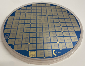
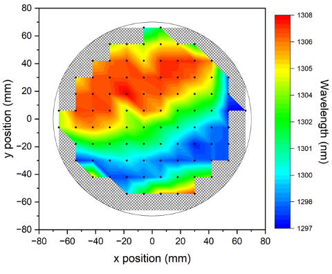
Figure 1. InAs QD EELs fabricated over 150- Figure 2: CW wavelength for 2 mm InAs QD devices, measured on wafer.
150 mm. In light of this, a quick fabrication approach has been developed for edge-emitting lasers (EELs). A fabricated EEL wafer is shown in Figure 1. On-wafer measurements, (for example Figure 2), can give great insight into quality and uniformity of the epitaxy. Full results for InAs QDs on GaAs have been disseminated at Photonics West 2023.

Wafer sizes are expected to fully transition to 200 mm for many applications. With the announcement of the first commercial 200 mm VCSEL wafer, work has been carried out to investigate performance on individual 200 mm GaAs and Ge substrate devices. Large amounts of wafer bow in these larger diameter wafers, can create a large oxidation extent variations.
The impact of this thermal oxidation non-uniformity on VCSEL performance was published earlier this year, comparing VCSELs grown on both GaAs and Ge substrates.
The first full 200 mm device wafer (Figure 3) has been processed in 2023, in the ICS facilities, by the Manufacturing Hub. Specific processes have been developed for dry etching, and p- and n-ohmic contacts for GaN LEDs, grown on Si substrates, with nominally 100% fabrication yield.