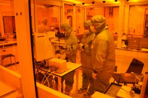
One of the key roles of the EPSRC Place Based Impact Accelerator Account (PBIAA) is to address the significant skills shortage for the rapidly expanding compound semiconductor industry. PBIAA has developed a week-long intensive training programme, designed and developed by the Institute for Compound Semiconductors (ICS), and recently delivered to engineering professionals from Semtech Corp, based in Bristol. The training programme utilised academic expertise from the CS cluster alongside local research infrastructure (Cardiff University’s Queen’s Training Cleanroom) to provide a combination of theory and practical training.
The training programme promoted the following outcomes:
- Understanding of the steps involved in fabricating an electronic semiconductor device;
- Knowledge of CS design, nanofabrication, and testing;
- Experience of the technologies and techniques used in fabricating a CS device;
- Knowledge of essential skills needed for working safely in cleanroom environments; and
- Practical exposure to semiconductor device processing.

Reflecting on the training undertaken, the staff who participated commented:
“The PBIAA skills course has helped me learn a lot about semiconductor processing, particularly relative to the III-V compound semiconductors, used often at Semtech. We looked principally at the etching and depositing processes, alongside the different issues/challenges encountered. The course has been incredibly useful to my professional development as I have re-learned processes, studied a long time ago at the start of my career, whilst also introducing me to new processes which I will need to consider in future.”
“My favourite part was operating the plasma etchers to etch patterns and sequels on the final wafers and seeing the process close up to fully understand how it worked. The course has broadened my knowledge and enhanced my understanding of the semiconductor processes, different to the silicon processes with which I am more accustomed. I’d recommend this training to anyone in or outside of the industry, especially graduate engineers who may not have been exposed to world of compound semiconductors.”
Further training courses are being rolled out according to partner requirements and include upcoming courses on Gallium Arsenide (GaAs) and also in crystal growth. PBIAA is currently offering training support to those cluster companies that are expanding so rapidly that it is challenging for them to meet their staff’s training needs and demands all by themselves.
Please contact us for more information and to see how we might help you